
Overview
The SQRL Forest Kitten 33 has a xcvu33p-fsvh2104-2L-e FPGA (which may be ES0/ES1 (engineering sample). I only have the air-cooled version, so I can only comment on it, but the fan blades are somewhat fragile. Regardless of this, the heatsink/fan combination is adequate, even under higher load situations. One thing of note is that it is extremely easy to disassemble - very few screws, which are easy to access.
Power Delivery
I am just learning about power delivery details myself - so the following is subject to change (and I make no guarantee about its correctness.)
The SQRL Forest Kitten 33 has only three power rails that most folks will want to modify - those being VCCINT (FPGA core power) with 120A (20x6) of 0.85V, HBM_VCC (ditto) with 20A of 1.2V, and VCCINT_IO with 20A of 0.85V (shown in some SQRL tools as VCCBRAM.) All three of these rails are modifiable using I2C programmable rheostats, which are basically a resistor one can modify the resistance of over I2C. Among the power rails which are not modifiable, there are 1.8V and 3.3V AUX supplies, both 6A, and the MGT supplies, which are 1.2V and 0.9V, also both 6A.
Controlling the voltages over I2C: This is a complex enough topic to warrant its own page, which is here.
My overall impression of the power delivery on this card is quite positive… for the VCCINT rail, anyhow. It does not suffer from being unable to supply all that the FPGA is capable of drawing - many FPGA boards, whether they were intended for mining or not, will lack the capability to give the FPGA VCCINT rail all the power that it can use under extremely high loads. This isn’t a problem here - we have 120A available on VCCINT, and according to Xilinx1, 120A is almost enough to max out an XCVU35P at 135A maximum, meaning there is PLENTY of headroom for a 33P. The HBM2 rail, however… is rather wimpy. The HBM_VCC rail is only rated for 20A at 1.2V. Exceeding this could damage the LTC7150S chip responsible for power delivery to the HBM2.
Changing the current capacity of the HBM_VCC rail would be an issue, because the FK uses a rather well-made part, the LTC7150S, but it’s made for really tiny boards with little room, basically. It’s good at what it does, but you won’t be able to replace it with most anything besides the same part, exactly - because it’s got internal FETs and shit. If it were a more normal setup, then yeah, maybe you could swap out some external FETs to get more current, but that ain’t flying here.
Clocking
SYSCLK is 200Mhz, and generated by an ASDMPLV-200.000Mhz, reaching the FPGA on pins AY23 and BC26 for SYSCLK_200_N and SYSCLK_200_P respectively. The PCIe reference clock is connected to AD9 and AD8 for the PCIe REFCLK_N and REFCLK_P, respectively. Note that these are MGTREFCLK pins.
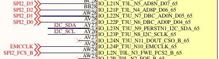
EMCCLK is generated by an ASDMB-125.000MHZ, on pin AV26, with a 1.8V supply. This allows for faster configuration speeds, compared to using the FPGA’s internal CCLK for configuration.
Board Interfaces and Peripherals
The FPGA has two flash devices, both of them Micron MT25QU256ABA8E12 256Mbit chips. The first one has SPI0_DQ0, SPI0_DQ1, SPI0_DQ2, and SPI0_DQ3 are wired to pins AW7, AV7, AW8, and AV8, and the chip select for it is SPI0_FCS at BA8.
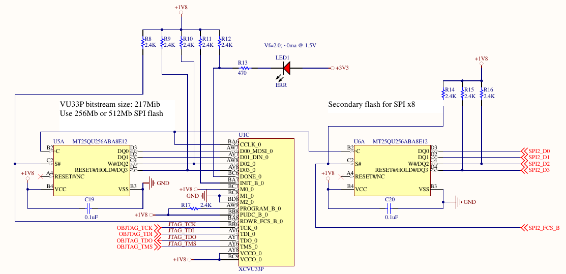
The second one has SPI1_DQ0, SPI1_DQ1, SPI1_DQ2, and SPI1_DQ3 at AV28, AW28, BB28, and BC28, respectively, and the chip select for it is SPI1_FCS at AW24. They can be used individually, or in dual-quad mode. Also, “Mib” in the above image is a typo, should be “Mb”.
-
Xilinx User Guide UG583 (Ultrascale Architecture PCB Design), Table 1-24: “Maximum VCCINT Current (A) (100°C, 10 Years)” ↩︎