
Basic Architecture
The E300 is a device with three seperate boards, each one with a Xilinx XCVU35P FPGA, which all are connected to a single control board with a Xilinx Zynq XC7Z010 via a ribbon cable with a 20-pin header. Zynq devices are FPGA devices with hard (ASIC) ARM CPU cores integrated onto the same chip - the dual-core ARM CPU responsible for running Linux and such, while the FPGA side offers access to the hardware on the FPGA boards through the Linux environment.
The Controller Board
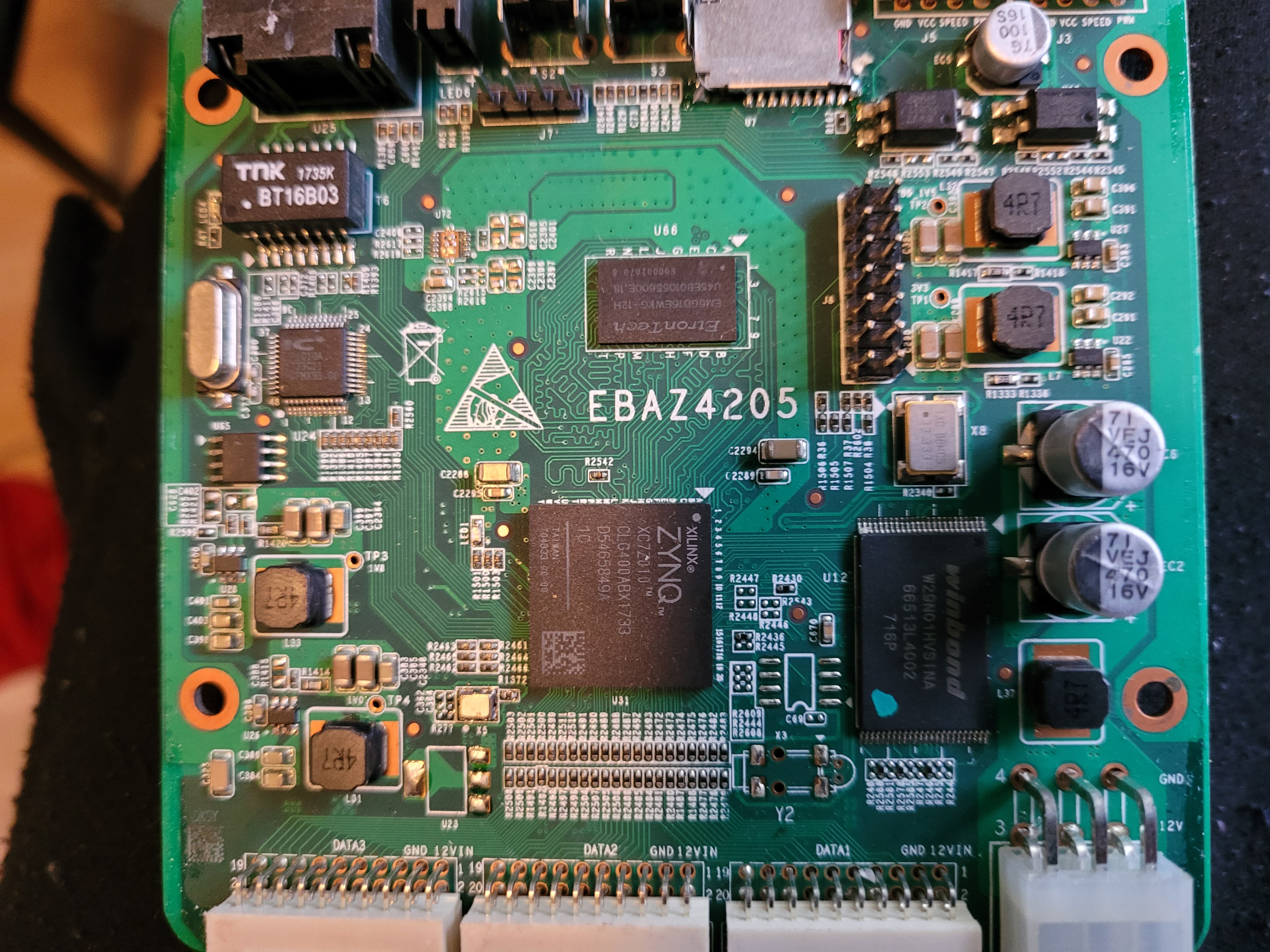
The Zynq controller board, the EBAZ4205, is based on the Xilinx Zynq XC7Z010. The FPGA side of this device is mainly to allow access to the hardware from the ARM cores under Linux. It has an Ethernet port, two fan headers, two buttons, and three plugs for 20-pin ribbon cables. Up to three FPGA boards may be connected via these plugs. For each FPGA board, there are JTAG lines, one UART (RX/TX only), and an I2C bus. Also connected to this header are several configuration-related FPGA pins, a pin to power-up or power-down the board, and several user I/O pins, one of which is intended to be used as a reset. All of these pins are connected to the FPGA side of the Zynq (often called the PL, for programmable logic.) A further note is that the JTAG and I2C lines have issues when being heavily used at the same time due to crosstalk.
The FPGA Board(s)
The FPGA board offers JTAG, UART, and I2C to the Zynq controller. JTAG allows configuration of the FPGA, and pretty much anything else you may want. The UART offers serial comms to a design flashed to the FPGA board. I2C has a bit more, however. The I2C bus offers access to some nice features of the FPGA boards, as well as providing us with more sensor information. The first of the devices is a TI TMP411C1 at I2C address 0x4E. It has two channels, the “local” channel is the board temperature, and the “remote” channel is for FPGA temperature. Next, we have the TI CDCE62142, a four-channel clock generator at 0x67 (normal mode) and 0x68 (fallback mode). The FPGA itself, the XCVU35P, of course, is also a slave on the I2C bus. I saved the best for last: the MP2975GU VRM controller at 0x7C. From this we can tune any and every aspect of power delivery if we like, from frequency of the buck, to slew rates, to the temps/currents/voltages which trigger OTP/OCP/OVP.
Interfaces
So, since the pins on the three boards are all connected to the FPGA side, how do we use them from the ARM side, on linux? Easy - Linux handles access to the variety of interfaces on each FPGA board via the “uio_pdrv_genirq” (UIO, or Universal I/O) driver, allowing us to access AXI registers on the FPGA portion of the Zynq using memory-mapped I/O. It simply creates a file in /dev with the name uioXY, and one can read/write to it normally. Now, we just need to know what registers there are, and what they do - thankfully, this is easier to find than it sounds. The interfaces go to Xilinx standard IP cores (except a few, which I will detail), which have all the AXI registers and usage details available via the usual Xilinx user guides for each IP core. If you recall, we have JTAG, UART, and an I2C bus available from every FPGA board. This gives us nine UIOs so far. There is one UIO to a custom IP core to control the fans (honestly, Xilinx’s AXI PWM probably would have been better, but I’ll take it), making for ten. There is another to control powering the boards up/down, so eleven, yet another UIO for reading the DeviceDNA (a unique identifier) from the Zynq board, for twelve, and finally, one last UIO, which is a custom AXI watchdog.
Connectivity
The FPGA board(s) are connected to the Zynq board via a 20-pin header. There are FPGA configuration signals which get passed to the Zynq board through here: CCLK, D01_DIN, PROGRAM_B, DONE, and INIT_B. If you don’t know what those are, don’t worry, it’s not that important. There are six user I/O pins, usable for whatever you like with your FPGA design (for the board) at AW14, AV20, AW19, AW18, AY17, and BE17. The last is intended to be used as an active-low reset. There is one pin to control power to the FPGA board (set high to power it.) Then there are the four JTAG pins (TCK, TDI, TMS, and TDO), UART pins (RX/TX), and I2C pins (SCL/SDA). There are three GND pins, and two pins are not used. That’s all twenty.